
0755-82760106
0755-83260671
Author:netwing Time:2024-04-24 Number Of Views:

Main features of LM393DR2G
Extremely low current drain, independent of power supply voltage, at 0.4mA
Input common mode range to ground level
The differential input voltage range is equal to the power supply voltage
Output voltage compatible with DTL, ECL, TTL, MOS, and CMOS logic levels
The ESD clamping at the input end improves the robustness of the device without affecting performance
Wide single power supply voltage range from 2.0VDC to 36VDC, and separated power supply range from ± 1.0VDC to ± 18VDC
Input offset voltage is ± 1.0mV typical value (TA=25 ° C, VCC=5.0VDC, ≤ thigh ≤ TA)
Voltage gain of 200V/mV typical value (RL ≥ 15k, VCC=15VDC, TA=25 ° C)
Large signal response time: 300ns (typical value) (Vin=TTL logic swing, Vref=1.4VDC, TA=25 ° C)
SOIC-8 package, operating temperature range: 0 ° C to+70 ° C
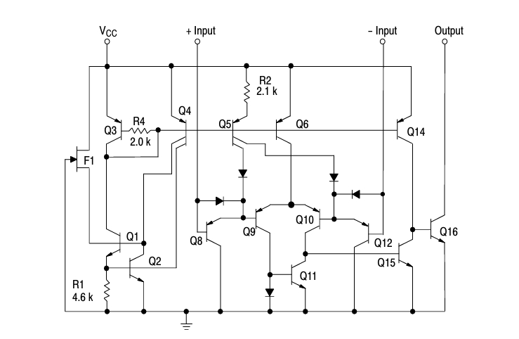
LM393DR2G is a LM393 series dual independent precision low offset voltage comparator that can achieve single or dual power supply. This device is designed to allow for a common mode range to ground level with a single power supply. The input offset voltage specification as low as 2.0mV makes this device an excellent choice for many applications in consumer electronics, automotive, and industrial electronics.
Previous Article:LM2901DR2G
Next Article:LM339DR2G
 Contact Us:0755-82760106
Proposal:0755-83260671
 Mailbox:jessie@ruizhengwei.com
 Address:18F, Building A, Rongde International, Henggang Street, Longgang District, Shenzhen City, Guangdong Province

Skype


Copyright © 2024 Shenzhen Ruizheng Microelectronics Co., Ltd Copyright Record number: Yue ICP Bei 2024178191-1 Background Login
 CH
CH EN
EN